

Growing atomically thin transistors on top of computer chips
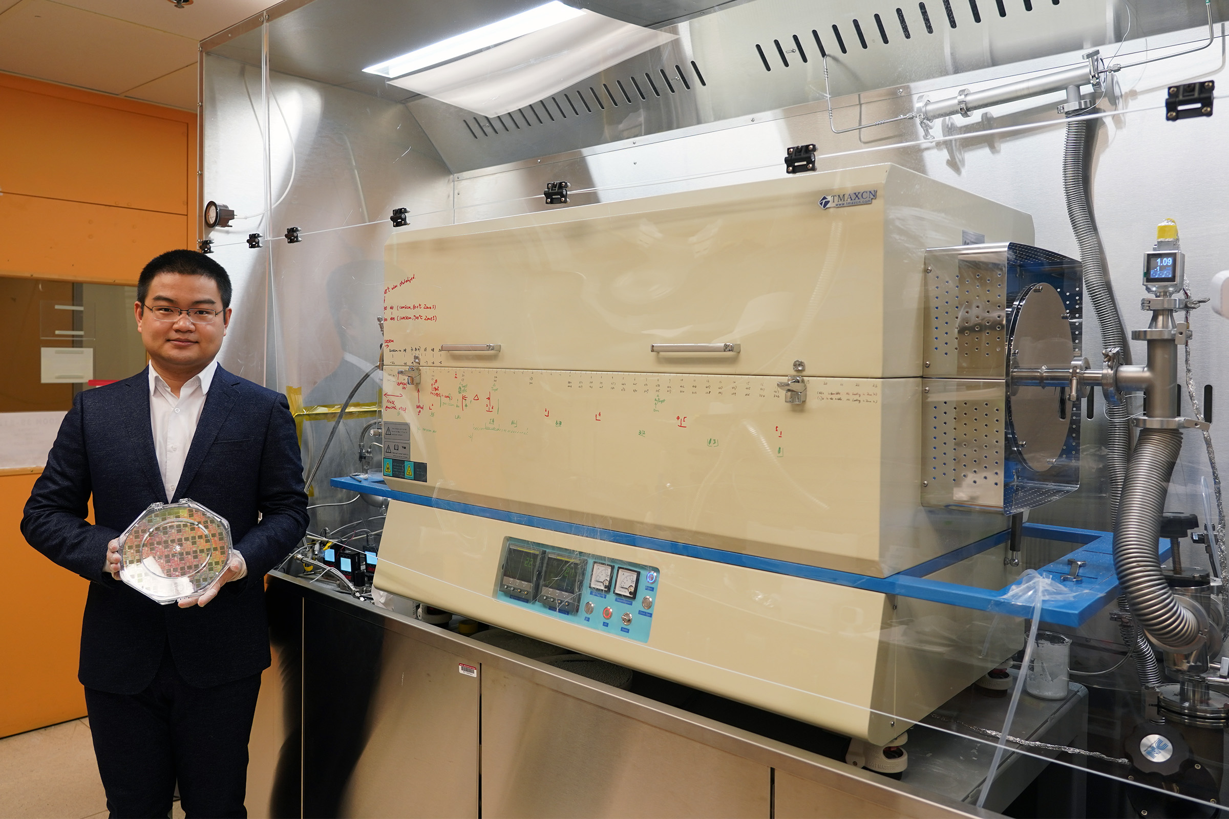
Graduate student Jiadi Zhu holding an 8-inch CMOS wafer with molybdenum disulfide thin film. On the right is the furnace the researchers developed, which enabled them to "grow" a layer of molybdenum disulfide onto the wafer using a low-temperature process that did not damage the wafer. Image: Courtesy of the researchers.
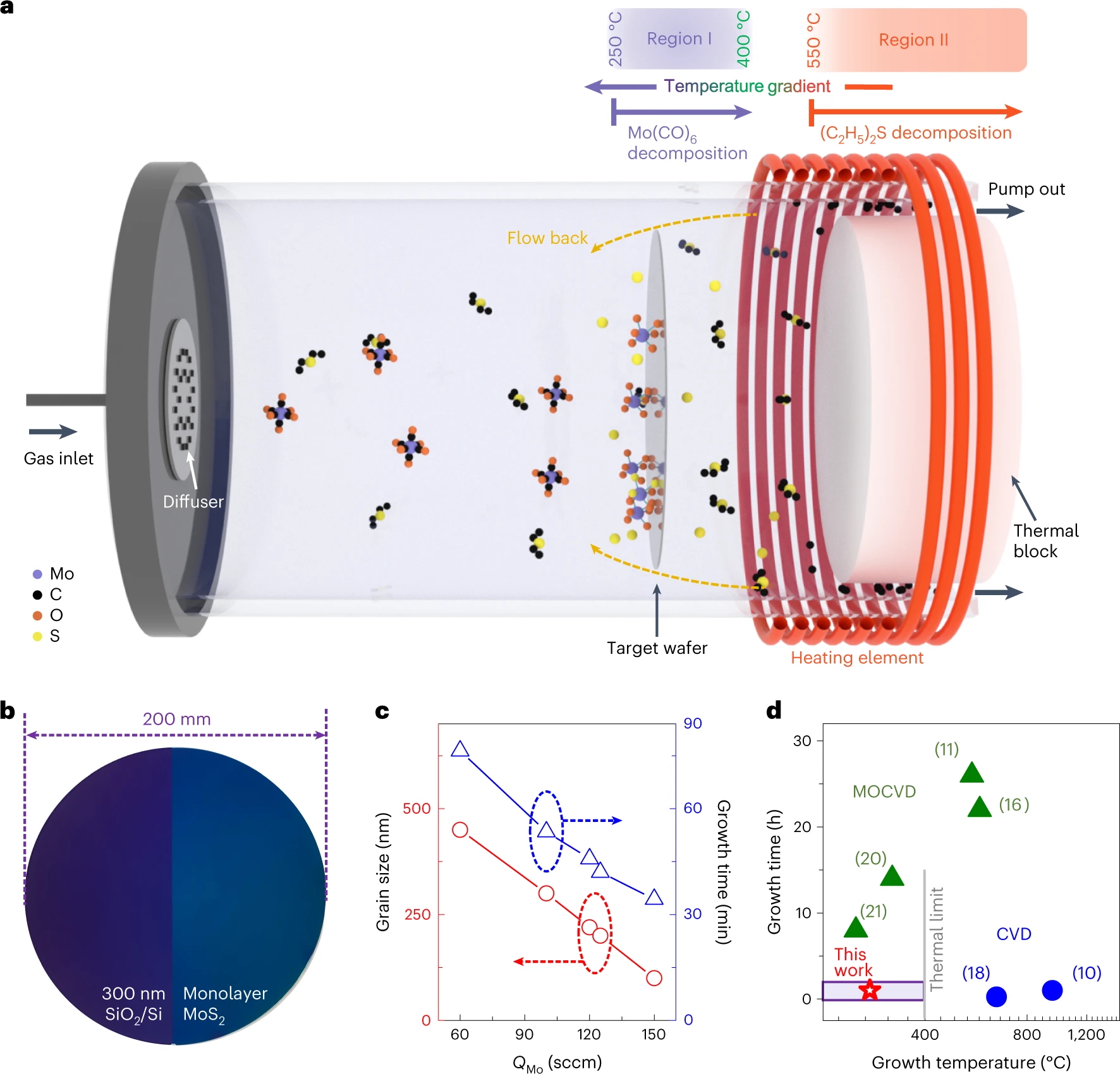
a, Schematic illustration of the MOCVD system and the deposition process. Precursors are injected from the left side of the reaction chamber. The molybdenum precursor starts to decompose on reaching the left side of Region I (250 °C). The sulfur precursor decomposes in Region II (>550 °C) and flows back into Region I where it reacts with the decomposed molybdenum precursor to deposit MoS2 on the target wafer. The residue gases are pumped out on the right side of the reaction chamber. A thermal block is placed in Region II to limit the gas flow. b, Optical image of MoS2 synthesized on top of a 300-nm-thick silica/silicon (SiO2/Si) substrate. The left half shows the bare 300 nm SiO2/Si substrate for comparison. c, Dependence of the growth time and grain size on the Mo(CO)6 flow rate (QMo) when the total flow rate is fixed at ~1,100 sccm. d, Benchmarking of thermal budgets for different synthesis methods of monolayer MoS2 growth. The purple rectangle indicates the desired region, and the number in parentheses indicates the reference number of the synthesis method. Image: Zhu, J., Park, JH., Vitale, S.A. et al. Low-thermal-budget synthesis of monolayer molybdenum disulfide for silicon back-end-of-line integration on a 200 mm platform. Nat. Nanotechnol. 18, 456–463 (2023).